
Voltage glitch turns an old mining card into a full 80 GB A100
A hardware researcher who goes by Kate used targeted voltage manipulation to break the burned-in locks on Nvidia’s GA100 chip. That turned a retired 8 GB CMP 170HX crypto-mining card into a fully usable A100 compute card with 80 GB of memory. In her tests, it even outperformed a retail A100.
What’s going on
A hardware researcher who calls herself only Kate on her blog published a detailed technical write-up on Tuesday titled “Using voltage glitching to unleash the A100 in my mining card”. In it, she describes a vulnerability in Nvidia’s GA100 chip, the GPU inside the well-known A100 data center card, among others. By tampering with the power supply at just the right moment during boot, Kate managed to bypass the chip’s electronic fuses, which determine which parts of the chip are usable.
The result: a CMP 170HX, a card Nvidia sold specifically for cryptocurrency mining that officially offers just 8 GB of memory, ran like an A100 with 80 GB of memory and all working compute units after the mod. That’s exciting for AI, because the A100 was the workhorse for training and inference of large language models for years, and used mining cards are much cheaper. Kate has published the technical details in the GA100VFI repository.
One chip, many products: how Nvidia bins with fuses
Nvidia builds different products from the same GA100 chip, from the pricey A100 for data centers to the CMP 170HX for mining farms. Out of the fab, every one of these chips has 128 streaming multiprocessors (the actual compute blocks), 12 framebuffer partitions (links to VRAM, the video memory), five NVDEC video decoding units, a PCIe Gen 4 x16 interface and several stacks of HBM. That’s High Bandwidth Memory: particularly fast memory stacked right next to the chip.
Which of these parts a product is actually allowed to use is decided by eFuses. These are tiny electronic fuses that get “blown” during manufacturing to lock in settings permanently. That’s how faulty areas of a chip get disabled and how products are kept distinct from each other. The odd part: a CMP 170HX 8 GB shows software only 8 GB of memory but carries around 80 GB of HBM on the package.
The GA100’s fuse controller manages 16,384 eFuses in 512 rows of 32 bits each. It reads them at boot, protects them and passes the resulting settings to the rest of the chip. Rows 0 to 221 hold regular fuses. Rows 222 to 487 hold so-called “fuseless fuses” (FF records). These entries are replayed in sequence, and a newer entry can overwrite the value of an older 16-bit block. That’s the crux: FF-backed options can be changed without having to undo a physically blown fuse. Rows 0 and 1 hold control fuses, including security-critical options.
FF entries also handle “floorsweeping”, the deliberate disabling of chip areas. Masks such as OPT_FBP_DISABLE, OPT_GPC_DISABLE and OPT_NVLINK_DISABLE determine which memory links, compute clusters and interfaces the GPU exposes. Earlier projects like cmpunlocker had already squeezed a bit more out of CMP cards with driver tweaks. Kate goes one level deeper, to the fuses themselves, which software couldn’t reach until now.
The attack: a precisely timed voltage hiccup
Kate’s method is called voltage fault injection, or voltage glitching. You briefly disrupt a chip’s supply voltage at exactly the right moment so that it executes instructions incorrectly. Think of a brief power flicker that distracts a bouncer at the exact moment someone slips past.
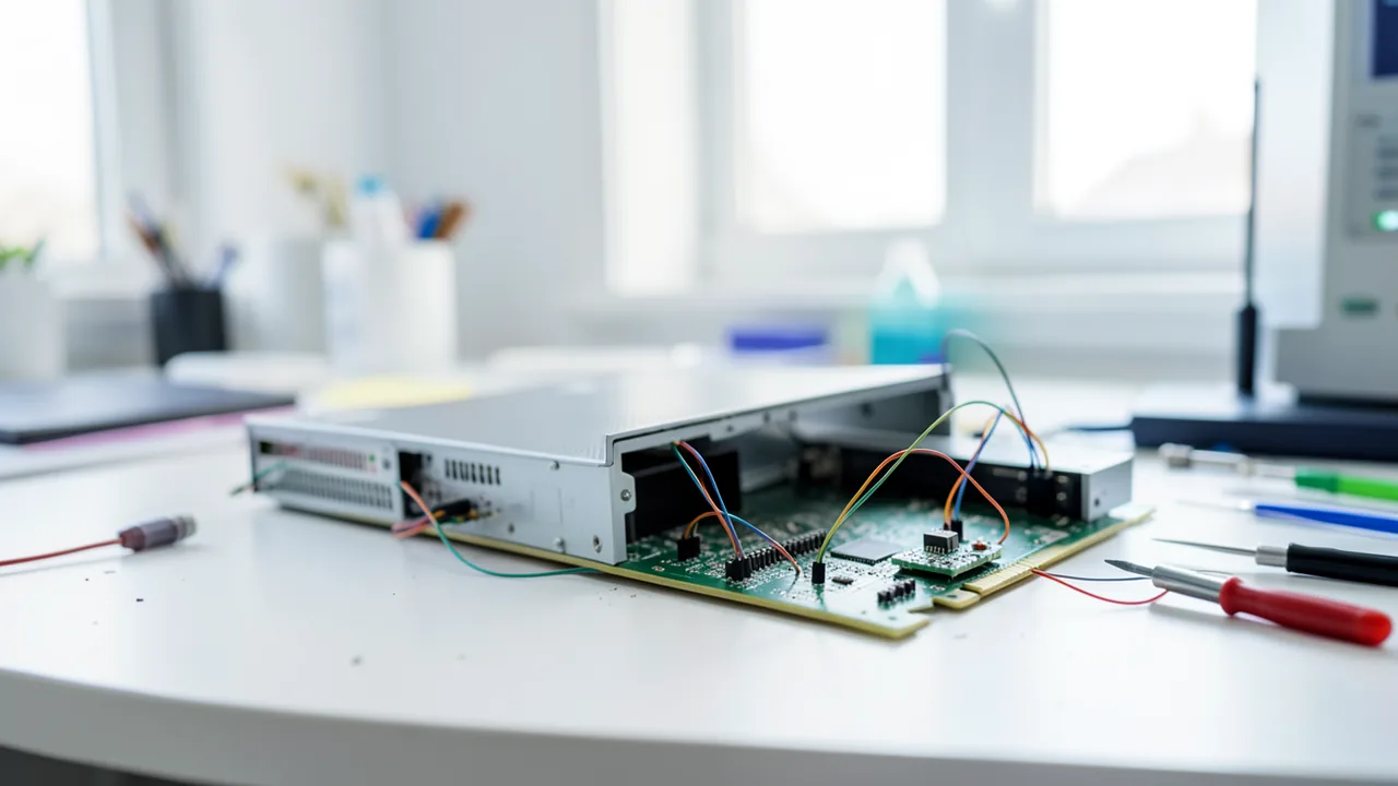
Specifically, Kate built a rig around an STM32G4 microcontroller board. It taps the PWMVID signal on the CMP 170HX’s board, the control signal the GA100 uses to tell the voltage regulator (an MP2888B) what voltage it needs. The board intercepts that signal and drives the regulator with precisely timed waveforms instead. The firmware triggers as soon as the core voltage NVVDD exceeds 225 millivolts and injects the glitches during boot. A host machine cycles the card back and forth between the ACPI S0 (on) and S3 (sleep) power states to allow many attempts in a row.
The experiments produced various fault states. Some left the settings values close to zero and the GPU unusable. The crucial state wiped the values in rows 0 and 1 but left all other fuse data intact. In that state, both DISABLE_SW_OVERRIDE and ENABLE_FUSE_PROGRAM were zero. A SENSE_CTRL command restored most control options, but not DISABLE_SW_OVERRIDE. That made software overrides possible. Kate then set OPT_SECURED_BURN_FEATURE_ENABLE to zero, adjusted privilege settings and wrote new FF rows in which the disable masks covered only the areas that were actually defective.
The benchmarks
In Kate’s tests, the modded card exposed the full 80 GB of HBM as usable memory, verified with synthetic read/write tests and real inference workloads. Compute performance took a clear jump:
| Card | FP16 FMA performance |
|---|---|
| CMP 170HX, software-unlocked | 50.129 TFLOP/s |
| Retail A100 | 72.488 TFLOP/s |
| CMP 170HX, hardware-unlocked | 85.861 TFLOP/s |
FP16 means computing with 16-bit floating-point numbers, as is common in AI training. FMA stands for fused multiply-add, the basic operation of neural networks. According to Kate, the modded mining card beat the retail A100 by a factor of 1.18. The summary doesn’t explain in detail why it’s faster than the original. The likely explanation is that all working streaming multiprocessors are active, whereas Nvidia disables some of them on the A100.
With the relevant locks removed, the card also ran at PCIe Gen 4. NVLink, Nvidia’s fast direct link between multiple GPUs, could be enabled too, but only with an extra firmware bypass and a bridge across pins of the U11 component footprint, which is unpopulated on the mining board. The video decoder (NVDEC), JPEG unit (NVJPG) and Multi-Instance GPU (splitting one GPU into several isolated sub-GPUs) appear unlockable the same way but weren’t tested.
Limits: not a weekend project
The mod is a lot of work and isn’t guaranteed to succeed. Of ten CMP 170HX cards examined, one had only 64 GB of working HBM instead of 80 GB, so the memory advantage shrank there. Every card needs its own FF entries tailored to its specific chip, because defects and used fuse space differ from unit to unit. In Kate’s setup, the glitching campaign took between one and 48 hours, and NVLink requires soldering on the board.
On top of that, Nvidia sold the CMP cards for mining and the A100 for data centers, with support, validation and warranty tied to those product definitions. Kate’s write-up shows what the hardware can do after a mod, not what works reliably in continuous operation.
The security angle and Nvidia’s response
Kate places her work in a growing line of physical attacks on GPUs and SoCs, citing among others Jon Pry’s work “A Canary in the Crypto Mine” and voltage glitching research on Nvidia’s Tegra chips. She says she informed Nvidia’s product security team before publishing, and that another researcher found the same flaw independently. The source doesn’t mention any public statement from Nvidia.
The real story is less the extra performance than the principle. Nvidia treats blown fuses as permanent. Yet thanks to the FF mechanism and the disrupted boot process, those limits could still be loosened on a production card. Kate points out that deeper fault states might also expose debug features or specially protected execution environments, and she plans to look into that next.
Our take
For the AI scene, this is mainly interesting as a proof of concept: retired mining cards apparently contain full-fledged A100 hardware, including 80 GB of fast memory. That’s exactly the resource that’s scarcest when you run large language models locally. But it’s only practical for very experienced hardware hackers with test equipment, a soldering iron and patience. This isn’t a how-to for everyone, and risks like instability or damaged cards remain. All benchmarks come from Kate’s own tests and haven’t been independently verified yet. For security teams, the message is clearer: on the GA100, eFuse-based product segmentation isn’t a hard security boundary once someone has physical access to the hardware. The write-up leaves open whether newer Nvidia chips like Hopper or Blackwell have similar weaknesses.
Sources
- Merkliste: news.lavx.hu news.lavx.hu
Ask the AI assistant
Questions about this article, installation or background? Our assistant knows this page and runs on our own machine, not in someone else's cloud.
The Assistant is an AI (Gemma 4) and can make mistakes – please check important details against the source. Questions are used only to generate an answer and are deleted after one hour. Please don't enter any personal data.



Comments
What do you think? Already tried it? Write it here, no sign-up needed.
Comments are public. Links aren't allowed, and we delete abusive posts. You can delete your own comment at any time in this browser. Learn more in the Privacy Policy.